| Sign In | Join Free | My himfr.com |
|

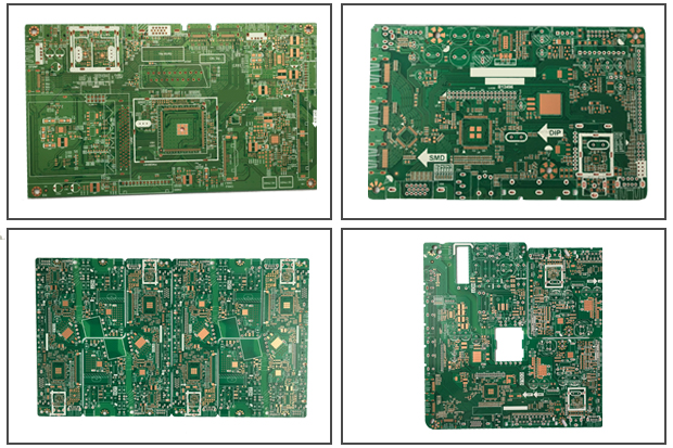
Shenzhen Lefang Electronics Co., Ltd
PCB Circuit Boards OEM ODM MAKE YOUR PRODUCT BETTER 18 Years Professional PCB Circuit Boards Supplier
Active Member
8 Years
- Home
-
Products
- PCB Circuit Board(32)
- FR4 PCB Board(40)
- Multilayer PCB Board(32)
- Double Sided PCB(28)
- Heavy Copper PCB(34)
- High TG PCB(19)
- Copper Base PCB(11)
- Single Sided PCB(7)
- High Frequency PCB(13)
- LED PCB Board(13)
- Medical Equipment PCB(16)
- Automotive Printed Circuit Board(19)
- Communication PCB(16)
- Industrial PCB(17)
- PCB Board Assembly(20)
- About Us
- Quality Control
- Contact Us
- Get Quotations